2
IR2171/IR2172
www.irf.com
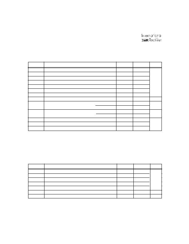
Symbol Definition
Min.
Max.
Units
V
S
High side offset voltage
-0.3
600
V
BS
High side floating supply voltage
-0.3
25
V
CC
Low side and logic fixed supply voltage
-0.3
25
V
IN
Maximum input voltage between V
IN+ and
V
IN-
-5
5
V
PO
Digital PWM output voltage
COM -0.3
VCC +0.3
V
OC
Overcurrent output voltage (IR2172)
COM -0.3
VCC +0.3
V
IN-
V
IN-
input voltage (note 1)
V
S
-5
V
B+ 0.3
dV/dt
Allowable offset voltage slew rate
50
V/ns
P
D
Package power dissipation @ T
A
d +25癈
8 lead SOIC
.625
8 lead PDIP
1.0
Rth
JA
Thermal resistance, junction to ambient
8 lead SOIC
200
8 lead PDIP
125
T
J
Junction temperature
150
T
S
Storage temperature
-55
150
T
L
Lead temperature (soldering, 10 seconds)
300
Absolute Maximum Ratings
Absolute maximum ratings indicate sustained limits beyond which damage to the device may occur. All voltage
parameters are absolute voltages referenced to COM, all currents are defined positive into any lead. The thermal
resistance and power dissipation ratings are measured under board mounted and still air conditions.
V
癈/W
W
Note 1: Capacitors are required between VB and Vin-, and between VB and Vs pins when bootstrap power is used. The
external power supply, when used, is required between Vs and Vin-, and between VB and Vs pins.
癈
Recommended Operating Conditions
The output logic timing diagram is shown in figure 1. For proper operation the device should be used within the recom-
mended conditions.
Symbol Definition
Min.
Max.
Units
V
B
High side floating supply voltage
V
S
+13.0
V
S
+20
V
S
High side floating supply offset voltage
0.3
600
V
PO
Digital PWM output voltage
COM
VCC
V
OC
Overcurrent output voltage
COM
VCC
V
CC
Low side and logic fixed supply voltage
9.5
20
V
IN
Input voltage between V
IN+
and V
IN-
-260
+260
mV
T
A
Ambient temperature
-40
125
癈
V
发布紧急采购,3分钟左右您将得到回复。
相关PDF资料
IR2172S
IC CURRENT SENSE 8SOIC
IR2175STR
IC CURRENT SENSE 0.5% 8SOIC
IR22771STRPBF
IC CURRENT SENSE 16SOIC
IRU3073CQTR
IC REG DL BCK/LINEAR 16-QSOP
ISL25700FRUZ-TK
IC TEMP SWITCH MFET DRVR 10TQFN
ISL6150IB
IC CTRLR HOT PLUG NEG VOLT 8SOIC
ISL6151IB-T
IC CTRLR HOT PLUG NEG VOLT 8SOIC
ISL6160CB-T
IC CTRLR BULK/AUXILIARY 14-SOIC
相关代理商/技术参数
IR2171STRPBF
功能描述:板上安装电流传感器 IR2171S is not recommended for new designs. RoHS:否 制造商:Honeywell 电流额定值:+/- 56 A 传感器/变换器类型: 电源电压:4.75 VDC to 5.25 VDC 响应时间:< 0.2 us 输出电压: 工作温度:- 40 C to + 85 C 准确性:+/- 0.24 % 频率范围:
IR2172
功能描述:IC CURRENT SENSING LINEAR 8-DIP RoHS:否 类别:集成电路 (IC) >> PMIC - 稳流/电流管理 系列:- 产品培训模块:Lead (SnPb) Finish for COTS
Obsolescence Mitigation Program 标准包装:50 系列:- 功能:电流开关 检测方法:- 精确度:±10% 输入电压:1.7 V ~ 5.5 V 电流 - 输出:600mA 工作温度:-40°C ~ 125°C 安装类型:表面贴装 封装/外壳:10-UFQFN 供应商设备封装:10-UTQFN(1.4x1.8) 包装:管件
IR2172PBF
功能描述:板上安装电流传感器 Linear Current Sensing IC in a 8-lead SOIC package RoHS:否 制造商:Honeywell 电流额定值:+/- 56 A 传感器/变换器类型: 电源电压:4.75 VDC to 5.25 VDC 响应时间:< 0.2 us 输出电压: 工作温度:- 40 C to + 85 C 准确性:+/- 0.24 % 频率范围:
IR2172S
功能描述:IC CURRENT SENSE 8SOIC RoHS:否 类别:集成电路 (IC) >> PMIC - 稳流/电流管理 系列:- 产品培训模块:Lead (SnPb) Finish for COTS
Obsolescence Mitigation Program 标准包装:50 系列:- 功能:电流开关 检测方法:- 精确度:±10% 输入电压:1.7 V ~ 5.5 V 电流 - 输出:600mA 工作温度:-40°C ~ 125°C 安装类型:表面贴装 封装/外壳:10-UFQFN 供应商设备封装:10-UTQFN(1.4x1.8) 包装:管件
IR2172SPBF
功能描述:马达/运动/点火控制器和驱动器 LINEAR CURRENT 600V SENSING IC RoHS:否 制造商:STMicroelectronics 产品:Stepper Motor Controllers / Drivers 类型:2 Phase Stepper Motor Driver 工作电源电压:8 V to 45 V 电源电流:0.5 mA 工作温度:- 25 C to + 125 C 安装风格:SMD/SMT 封装 / 箱体:HTSSOP-28 封装:Tube
IR2175
功能描述:IC CURRENT SENSE 0.5% 8DIP RoHS:否 类别:集成电路 (IC) >> PMIC - 稳流/电流管理 系列:- 产品培训模块:Lead (SnPb) Finish for COTS
Obsolescence Mitigation Program 标准包装:50 系列:- 功能:电流开关 检测方法:- 精确度:±10% 输入电压:1.7 V ~ 5.5 V 电流 - 输出:600mA 工作温度:-40°C ~ 125°C 安装类型:表面贴装 封装/外壳:10-UFQFN 供应商设备封装:10-UTQFN(1.4x1.8) 包装:管件
IR2175PBF
功能描述:马达/运动/点火控制器和驱动器 Lin Cur Sens IC RoHS:否 制造商:STMicroelectronics 产品:Stepper Motor Controllers / Drivers 类型:2 Phase Stepper Motor Driver 工作电源电压:8 V to 45 V 电源电流:0.5 mA 工作温度:- 25 C to + 125 C 安装风格:SMD/SMT 封装 / 箱体:HTSSOP-28 封装:Tube
IR2175S
功能描述:IC CURRENT SENSE 0.5% 8SOIC RoHS:否 类别:集成电路 (IC) >> PMIC - 稳流/电流管理 系列:- 产品培训模块:Lead (SnPb) Finish for COTS
Obsolescence Mitigation Program 标准包装:50 系列:- 功能:电流开关 检测方法:- 精确度:±10% 输入电压:1.7 V ~ 5.5 V 电流 - 输出:600mA 工作温度:-40°C ~ 125°C 安装类型:表面贴装 封装/外壳:10-UFQFN 供应商设备封装:10-UTQFN(1.4x1.8) 包装:管件
